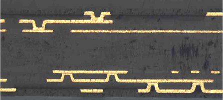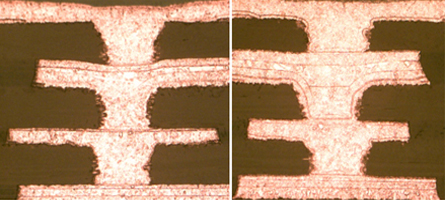

HDI PCBs always contain laser & NC drilling blind vias, buried vias, stack vias, stager vias, skip vias, step vias, through holes, fine lines and spaces, sequential lamination, Via-in-Pad technology and often with microvias diameter not more than 6mil, and etc.
HDI PCB Manufacturing Capabilities:
|
Item |
Typical Value |
Advanced Production |
|
Layer Count |
4-16 Layers |
4-24 Layers |
|
PCB Thickness |
0.6-1.0mm |
0.6-3.2mm |
|
Buid Up Technology |
I+N+I (i≥1) |
Any layer innterconnected |
|
Min. Laser Drilling Diamter |
4mil (0.1mm) |
3mil (0.075mm) |
|
Laser Technology |
CO2 Laser Machine |
CO2 Laser Machine |
|
Glass Transition (Tg) |
130/150/170°C |
130/150/170°C |
|
Hole Copper |
12-18μm |
12-18μm |
|
Impedance Control |
+/-10% |
+/-7% |
|
Layer to Layer Registration |
+/-3mil |
+/-2mil |
|
Solder Mask Registration |
+/-2mil |
+/-1mil |
|
Min. Trace Width/Spacing |
3/3mil |
2.0/2.0mil |
|
Min. Annular Ring |
2.5mil |
2.5mil |
|
Min. NC Drilling Diameter |
8mil (0.2mm) |
6mil(0.15mm) |
|
Min. Micro Via |
4.0mil |
3.0mil |
|
Min. Build-up Dielectric Thickness |
3.0mil |
2.0mil |
|
Max. Micro Via Pad |
12mil |
10mil |
|
Max. Micro Via Aspect Ratio |
0.8:1 |
1:1 |
HDI Boards Design Rules:
|
Item |
Capability |
Advanced |
|
Base Copper |
9-18μm |
3-18μm |
|
Min. Trace Width for Outer Layer |
3mil |
2.5mil |
|
Min. Trace Spacing for Outer Layer |
3mil |
3mil |
|
Min. Trace Width for Inner Layer |
3mil |
3mil |
|
Min. Trace Spacing for Inner Layer |
3mil |
3mil |
|
Microvia Size |
4mil (0.1mm) |
3mil(0.075mm) |
|
Min. Microvia Landing Pad |
Microvia Size + 8mil(0.2mm) |
Microvia Size + 6mil(0.15mm) |
|
Min. Microvia Pad |
Microvia Size + 8mil(0.2mm) |
Microvia Size + 8mil(0.2mm) |
|
Min. NC Drilling Diameter |
8mil(0.2mm) |
6mil(0.15mm) |
|
Min. Pad Size |
Drilling Size + 12mil(0.3mm) |
Drilling Size + 10mil (0.25mm) |
|
Dielectric Thickness |
2-4mil |
2-5mil |